EUV application upgrades, SK Hynix 1c DRAM progresses to the sixth level

SK Hynix is accelerating the promotion of 1c (sixth generation 10nm level) DRAM technology, planning to increase EUV exposure levels to level 6, and then improve product performance and yield.
Currently, the three largest memory manufacturers in the world are investing in the 10-nanometer advanced DRAM process. Samsung claims to have successfully broken through the yield rate of the sixth-generation (1c) DRAM, reaching more than 50%. After Micron released the 1γ (Gamma) advanced process, it has delivered the 1γ DDR5 samples to major customers such as Intel and Ultramicro (AMD) for verification in February this year; while SK Hynix announced last year that it had completed the development of the 1c process DDR5, and was the first to compete with its competitors to enter the advanced process.
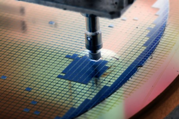
SK Hynix will increase EUV application, mainly because its wavelength is only 13.5 nanometers, which can engrave more detailed circuit patterns on the wafer and reduce multiple exposure steps, which will play a key role in improving DRAM density, speed and energy efficiency. The expansion of EUV layer data to level 6 means that more key processes will adopt this technology, which will not only help improve production yields, but also achieve more refined and stable line production. In contrast, Micron's 1γ DDR5 uses only one layer of EUV mask, which reduces EUV usage to reduce production costs, in a clear contrast with SK Hynix's high-level strategy.
With the continuous maturity of 1c process and EUV technology, the market is expected to usher in DDR5 memory products with larger capacity, faster speed and higher energy efficiency. Not only can meet the demand for high-speed memory by high-performance computing (HPC), artificial intelligence (AI) servers and data centers, but it will also promote performance upgrades for high-level PCs and workstations. At the same time, as these applications continue to increase their memory performance and energy efficiency requirements, DRAM processes are expected to further improve their dependence on EUVs, and manufacturers must introduce the technology in more key layers to pursue higher performance and smaller sizes, and promote the penetration and popularity of EUVs in advanced processes.
SK Hynix Reportedly Ramps 1c DRAM to Six EUV Layers, Setting the Stage for High-NA EUV Designs to Give Samsung No Chance of Competition


